


Within industrial environments, there are numerous cases where galvanic isolation of circuit parts is required. The useful signals can be transmitted capacitively, inductively or optically across an isolation barrier. The following example circuit shows how capacitive digital isolators can be used to electrically isolate remote industrial devices.
Interference-free data communication and personal safety are two major challenges for electronics in typical industrial environments. Strong electromagnetic fields, overvoltages, transient voltages and high electromagnetic compatibility (EMC) interference are the order of the day. If, for example, the communication cable is laid unfavorably close to a control cable of a frequency inverter, the pulses are capacitively coupled and the signals in the communication cable oscillate with the pulse pattern of the frequency inverter. This interference can quickly reach a level where significant malfunctions can occur and even endanger the safety of people.
For example, when the temperature of a motor is measured with a thermocouple, voltages in the millivolt range are generated. If these voltages are now transmitted over a cable length of several meters to a central control unit that refers to a different Earth potential, the measurement signal is distorted by the potential differences.
If we summarize the phenomena described above, the following four challenges arise:
- Safety barrier between hazardous voltages and users
- Separation of ground loops between spatial circuits
- Minimization of common-mode interference
- Interference-free data transmission
Figure 1 shows the situation of the data transmission system graphically. To meet the requirements of shielding dangerous voltages from the user and still guarantee interference-free data transmission, galvanic isolation must be implemented that separates the zones electrically—i.e., in terms of potential—so that they can work separately and thus without interference. The data flow runs via the digital isolator. However, interference and potential equalization currents are prevented by galvanic isolation.

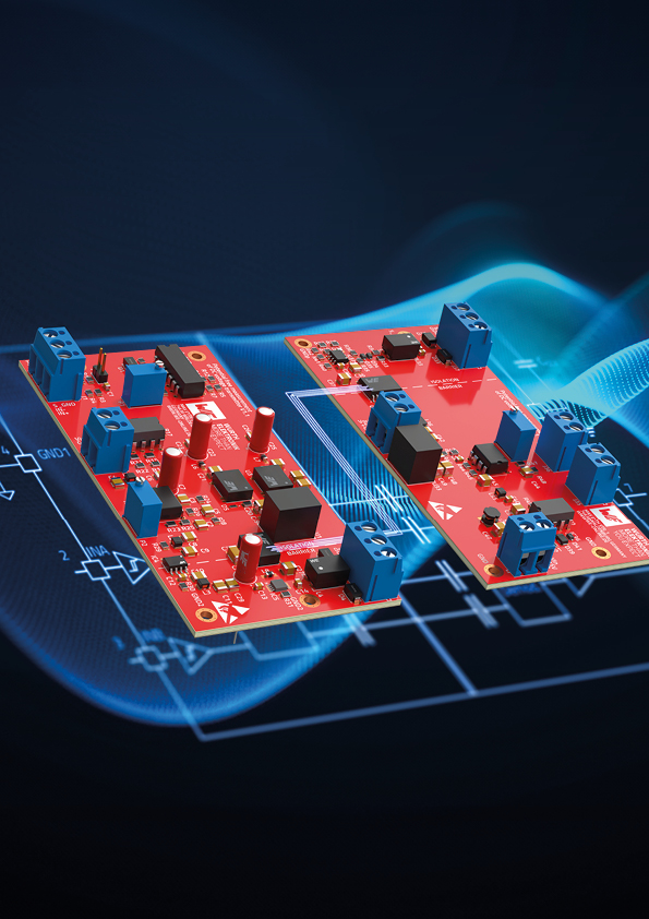
Isolated measurement of a battery voltage
The decentralized recording of physical parameters is the current state of the art. However, recording the data on the object is often a challenge, and wireless transmission of the data is frequently not possible. The data must be recorded on the object in such a way that the probe does not influence the variable to be measured; otherwise, measurement errors will occur. This requires electrical decoupling, which must be implemented in the circuitry. Furthermore, the wired transmission of the data must be potential-free and symmetrical so that the transmission is not disturbed by electromagnetic coupling and ground loops. In this application, the use of microcontrollers was deliberately avoided to demonstrate that a powerful, interference-free design can be implemented with little effort using analog circuit technology.
The design is divided into two circuits: a transmitter and a receiver. The transducer can detect a DC voltage of ±30 Vmax with a fluctuation period of one second. The current consumption has been minimized and, with a power supply of 15 V, is <85 mA for the transmitter and <25 mA for the receiver. Both the transmitter and the receiver are electrically isolated—the transmitter between the measurement data acquisition and the signal transmission path, and the receiver between the signal transmission path and the data output. Special DC/DC power modules and digital isolators with galvanic isolation and particularly low parasitic coupling capacitance were used to achieve this isolation in the circuitry. The signal is transmitted between the transmitter and receiver via a two-wire cable. Depending on the electromagnetic environmental influences, the distance can be several hundred meters.
Transmitter circuit design
Figure 2 shows the block diagram of the transmitter. The circuit is divided into six blocks:
- Probe: Measuring transducer with a voltage divider and amplifier for measuring positive and negative polarity (1)
- Level shifter: Level shifter for the voltage-to-frequency converter (2)
- Voltage-to-frequency converter: Digital output signal, frequency dependent on the input voltage (3)
- Digital isolator: Galvanic isolation between measuring potential and interface (4)
- Interface buffer: Low-impedance line driver with balanced output (5)
- Power supply: DC/DC converter, galvanically isolated converters for the probe head section (6)
To ensure functional reliability, measures for transient protection and filters are provided both on the probe side and at the driver output; low-pass filters are also provided before and after the DC/DC power modules to effectively attenuate RF coupling.

Receiver circuit design
Figure 3 shows the block diagram of the receiver. The circuit is divided into five blocks:
- Input buffer: Signal pickup, signal conditioning with balanced input. The link detector indicates whether there is a detectable connection to the transmitter (1).
- Digital isolator: Galvanic isolation between input signal and secondary signal processing/output interface. Additional galvanically isolated voltage for the input-side buffer (2).
- Frequency-to-voltage converter: Generates an output voltage from a digital signal. The voltage level depends on the frequency of the input signal (3).
- Interface buffer with polarity display: Level converter for the output signal. The output signal has a positive polarity, the polarity indicator shows the polarity of the input signal (4).
- Power supply: DC/DC converter for the secondary supply (5).
Numerous EMC measures are also provided in the receiver section. The signal input coming from the twisted-pair cable is equipped with transient protection and a common-mode filter to effectively attenuate interference coming from the cable. The power supplies around the DC/DC converters are equipped with low-pass filters on both the input and output sides to significantly reduce electromagnetic interference from both outside and inside the circuit caused by the switching operations of the DC/DC converters. This ensures a high signal-to-noise ratio and a high level of functional reliability.

Capacitive digital isolators
The digital isolator from Würth Elektronik1,2 consists of an oscillator and a modulator on the primary side. A demodulator and a signal buffer are located on the secondary side. The components on the primary side are electrically isolated from the components on the secondary side by a capacitive structure with an isolation barrier made of SiO2. The signal is transmitted across the isolation barrier using a modulation process known as on-off keying (OOK). The oscillator integrated into the chip is used to modulate the input signal, which runs via a Schmitt trigger. The modulator generates a differential signal that is transmitted via the capacitive insulation lines.
Two communication structures have become established in the world of digital isolators: edge-based and OOK. In principle, they can be regarded as equivalent methods. However, depending on the application requirements, the differences between the two architectures can influence the decision.
With the edge-based architecture, the input and output states are no longer sampled as soon as a data signal is activated. In the event of a power failure or failure of the data signal, this behavior can lead to an error. Therefore, the edge-based method requires an integrated refresh circuit to minimize the risk of errors under these conditions and to amplify the input state at the output.
With OOK, the input variable is continuously sampled and transmitted via the isolation barrier. Due to the continuous sampling of the input, no errors will show in the output in the event of an unintentional change in the supply or the input signal. With OOK, no additional refreshing circuits are required as with edge-based.
The first difference between the two methods is therefore energy consumption. An edge-based architecture consumes less energy, as it is sampled only once, whereas OOK requires permanent energy.
The second point of differentiation is that the OOK modulation scheme offers inherent advantages in terms of noise and transient behavior with a much higher CMTI and the added benefit of higher data rates due to continuous sampling.
Summarized:
- Edge-based architecture: Fewer losses and lower data rate
- On-off keying: Failsafe behavior, improved CMTI and more robust noise behavior
Figure 4 illustrates the circuit blocks. The demodulator, on the secondary side of the isolator, performs the functions of amplification, filtering and reconstruction of the input signal. The signal delay and signal distortion are minimized. Finally, a buffer routes the signal from the demodulator output to the overall output, whereby the buffer amplifies the signal to the required level.

Safety first! In an emergency, the digital isolators should protect people from dangerous voltages.
They must therefore fulfill the highest safety and durability requirements. The digital isolators of the CDIP and CDIS series from Würth Elektronik have been certified by the VDE in Germany according to the latest and most demanding standard, DIN EN IEC 60747-17 (VDE 0884-17):2021-10 “Magnetic and capacitive couplers for basic insulation and reinforced insulation” (see Table 1).
| Parameter | IEC 60747-17 (VDE 0884-17) | |
| Basic Isolation | Reinforced Isolation | |
| Package | SOIC-8NB | SOIC-16WB |
| VIOSM (max. surge isolation voltage) | 5,000 Vpk | 7,070 Vpk |
| Test | VTEST = 1.3 × VIOSM VTEST = 6.5 kV |
VTEST = 1.6 × VIOSM VTEST = 11.3 kV |
| Failure rate over lifetime | ≤1,000 ppm | ≤1 ppm |
But what do the terms “basic” and “reinforced” mean for a person’s safety? The standard itself only gives a rather abstract definition here—see IEC 60747-17:202X:
When do we choose basic—or reinforced—isolation? Put simply, the points “single fault condition” and “normal operating conditions” are important here. Reinforced insulation guarantees protection against electric shock even under single-fault conditions in normal operation. Basic insulation is only effective in normal operation, i.e., without consideration of a single fault.
Linear transfer characteristic
Figure 5 shows the relationship between the measured voltage and the voltage that is then displayed at the output. The transfer characteristic is almost linear over the entire input voltage range from –30 V to 30 V. The shown design consisting of a transmitter and receiver PCB connected via a twisted-pair cable is therefore a suitable solution for galvanically isolated data acquisition and transmission.
